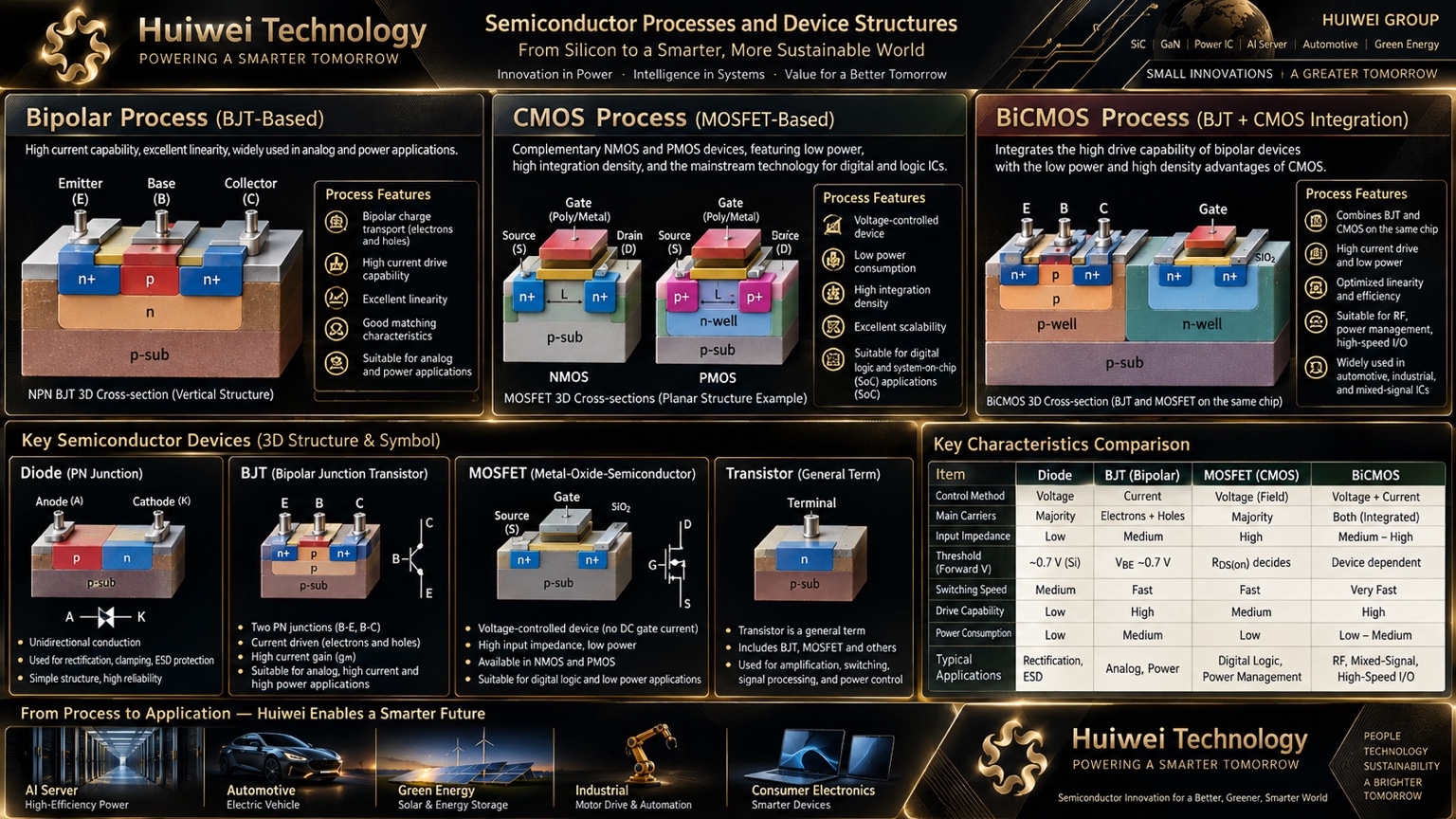
From process platforms to power applications: understanding Bipolar, CMOS, BiCMOS, Diodes, BJTs and MOSFETs.
Bipolar, CMOS and BiCMOS describe fabrication and integration platforms. Diodes, BJTs and MOSFETs are device types. Transistor is a general term that includes BJTs and MOSFETs. Si, SiC and GaN are semiconductor materials—a separate classification.
Three process platforms
Bipolar Process
Built around NPN and PNP BJTs, using electrons and holes in conduction. Bipolar devices can offer high transconductance at a given bias current for analog amplification, precision signals and drive circuits. Bias, noise, power and bandwidth remain design trade-offs.
CMOS Process
Integrates complementary NMOS and PMOS devices on one chip. Complementary logic enables low static power and dense digital integration; leakage and switching power still matter. CMOS is not the fabrication process for every discrete power MOSFET.
BiCMOS Process
Integrates BJTs and CMOS on one chip. Circuit designers can combine bipolar analog and drive performance with CMOS logic and high input impedance for mixed-signal, RF and interface applications. Results depend on the process and circuit.
Device functions compared
Item
Diode
BJT
MOSFET
Terminals
Anode / Cathode
Emitter / Base / Collector
Gate / Source / Drain
Control & conduction
Terminal voltage determines I–V behavior; no independent control terminal
VBE sets collector current; sustained base current is generally required
VGS controls the channel; switching requires gate-charge current
Typical roles
Rectification, clamping and protection, depending on device design
Amplification, biasing, signals and current drive
Logic, power switching and conversion
Selection criteria
Blocking voltage, VF, current, recovery and thermal resistance
Voltage, gain, SOA, bandwidth and thermal resistance
Voltage, RDS(on), Qg, losses, SOA and thermal resistance
Huiwei 3D process concept illustration
Conceptual teaching illustration, not a verified foundry cross-section or product specification. Some graphic labels and rankings are simplified or inaccurate; use the technical clarifications below and official datasheets.
Original English visual, shared by both language editions. Select the image to view full resolution.
Technical clarifications for this illustration
The main NPN E–B–C regions are n–p–n; PMOS p+ source/drain regions reside in an n-well. The illustrated doping, contacts and BiCMOS section are not a fabrication layout.
RDS(on) is on-resistance, not the threshold voltage VGS(th). Threshold marks the onset of channel conduction; full enhancement requires the datasheet-specified gate drive.
A MOSFET draws very little steady gate current, but switching requires drive current. BJT current gain β and transconductance gm are different parameters.
A silicon PN diode does not have a fixed 0.7V drop. Schottky diodes use a metal–semiconductor junction. Huiwei SiC Schottky diodes must not be modeled from the silicon PN sketch or a 0.7V assumption.
Speed, power, drive capability and input impedance cannot be ranked by device name alone. Compare operating point, process, circuit, load and temperature. BiCMOS is an integration platform, not a single device with fixed terminals or a universally fastest rating.
From device physics to Huiwei power applications
Huiwei focuses on SiC power devices while evaluating GaN for high-frequency conversion. Device selection for AI server power, 800VDC, energy storage and industrial power must consider topology, voltage margin, switching and conduction losses, gate drive, thermal design and reliability. This process overview does not imply that Huiwei offers every process or device described.
From process platforms to power applications.
Bipolar, CMOS and BiCMOS describe how devices are integrated on a chip. Diodes, BJTs and MOSFETs describe how devices operate. BJTs and MOSFETs are both transistors; Si, SiC and GaN are material choices.
Understanding these distinctions connects device selection to efficiency, gate drive, thermal design and reliability. Huiwei focuses on SiC power devices while evaluating GaN for high-frequency conversion, addressing AI server power, 800VDC infrastructure, energy storage and industrial power.
Huiwei Technology — Powering a Smarter Tomorrow.
#HuiweiTechnology #Semiconductor #SiC #GaN #MOSFET #BiCMOS #PowerElectronics #AIServer #800VDC
 Huiwei Technology